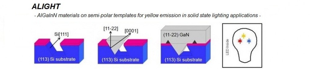
Gallium nitride (GaN) based crystals are the construction materials for the light emitting diodes (LEDs) that have caused a revolution in lighting, due to their superb efficiency, compactness and long lifetime. Present LEDs are based on a polar crystal orientation which is theoretically not ideal, but readily available. The ALIGHT project sought to develop scalable processes for the growth of GaN layers with a semipolar crystal orientation and demonstrate their use in LED devices. This semipolar orientation should lead to higher efficiency, higher switching speeds, and excellent polarization characteristics. The project ran from June 2012 to May 2015 with a consortium of 6 members consisting of the Tyndall National Institute (Ireland), the University of Cambridge (UK), the University of Ulm, MPIE, FBH and OSRAM (all in Germany). Through strong collaboration, the consortium successfully developed large (100 mm diameter) wafers with semipolar GaN layers, that served as templates for the growth of semipolar LED structures. LEDs with excellent performance for the early stage of development were demonstrated and the first 100 mm diameter semipolar LED wafer was processed on an industrial manufacturing line. These templates, which may be used to develop new types of sensors and electronic devices as well as LEDs, are ready for the next stage of development.
ALIGHT
AlGaInN materials on semi-polar templates for yellow emission in solid state lighting applications